

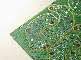
testing pcb hdi
The use of high-density interconnects (HDI) on printed circuit boards (PCBs) enables more components and connections to fit into smaller spaces than conventional PCBs. The advantages of HDI include reduced weight, higher reliability, and increased performance. However, there are also some challenges that can arise, such as signal integrity and electromagnetic interference (EMI). Proper design practices and rigorous testing can mitigate these risks and ensure successful and robust implementations of HDI.
pcb hdi can be found in a variety of electronic devices that require high-performance while conserving space, including touch-screen devices, mobile phones, 4/5G network communications, digital cameras, and military applications. Due to the advanced technology and small size of these devices, they require high-speed signals that may produce heat, requiring effective thermal management strategies.
Optimal component placement is crucial to ensuring effective signal integrity and EMI mitigation. This can be achieved through proper impedance control, ground planes, and shielding techniques. It is also critical to optimize trace widths and spacing to reduce signal crosstalk, EMI, and impedance mismatches.
What challenges exist in testing pcb hdi?
Insufficient clearance between components can result in mechanical stress on the interconnects. This can cause signal degradation or a breakdown of the connection. In addition, signal integrity issues can arise from poor routing paths. This can be prevented by using differential pairs, length matching, and careful planning of routing routes.
The high density of the PCB can lead to thermal problems. This can be addressed by properly designing the stack-up and using thinner dielectric layers to separate ground and power planes. In addition, it is important to consider the placement of heat-generating components and to use copper fills for improved thermal dissipation.
Manufacturing complexities can lead to issues during assembly and soldering. These challenges can be minimized by collaborating closely with the manufacturer and following design for manufacturability guidelines. Additionally, implementing effective simulation tools to evaluate and test the HDI design is crucial.
Numerous design rules: Due to the many parameters and interdependencies of HDI designs, they are more complicated to verify for compliance than traditional PCBs. Moreover, these rules are constantly evolving and may conflict with each other, making it difficult to maintain compliance throughout the entire design process.
PCB Material Selection: The choice of core and prepreg materials has a significant impact on the manufacturing cost of HDI PCBs. This includes factors like core thickness, layer stack-up, and the number of sequential laminations required. Choosing the right material can reduce the overall cost of the board while maximizing its function and quality.
The complex nature of the PCBs requires thorough and meticulous inspection to prevent errors and defects. Failure to do so can lead to expensive repairs or even product failure. Therefore, it is imperative to use the best PCB supplier that offers a wide range of testing services and provides a reliable quality guarantee. In addition, PCB suppliers should offer fast turnaround times and efficient customer service to improve their value proposition.