

stencil design for Pcb rigid flex
Optimizing stencil design for PCB (Printed Circuit Board) rigid flex is essential for ensuring the efficient production and performance of electronic devices. Rigid-flex PCBs offer unique advantages, such as improved reliability, reduced assembly time, and enhanced design flexibility. However, achieving optimal stencil design for such boards requires careful consideration of various factors to ensure successful manufacturing processes and high-quality end products.
One crucial aspect of optimizing stencil design for pcb rigid flex is understanding the specific requirements and constraints of the rigid-flex PCB architecture. Unlike traditional rigid PCBs, rigid-flex PCBs incorporate both rigid and flexible materials, allowing for complex three-dimensional configurations. Therefore, stencil design must accommodate the flexibility and bending capabilities of the flex regions while maintaining the structural integrity of the rigid portions.
The first step in optimizing stencil design is to accurately define the pad and aperture geometries based on the component footprints and assembly requirements. Properly sized apertures ensure precise solder paste deposition onto the pads during the assembly process, facilitating reliable electrical connections and minimizing defects such as solder bridging or insufficient solder joints. Additionally, optimizing the stencil thickness and material properties is crucial for achieving consistent paste release and maintaining stencil durability throughout multiple assembly cycles.
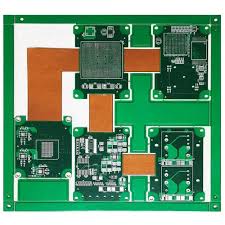
How do you optimize stencil design for Pcb rigid flex?
Furthermore, considering the unique challenges posed by rigid-flex PCBs, such as varying thicknesses and material properties across the board, it’s essential to tailor the stencil design to accommodate these differences effectively. This may involve adjusting the aperture sizes and shapes to compensate for variations in solder paste volume requirements due to differences in substrate thickness or material composition.
Another critical factor in stencil optimization for PCB rigid flex is ensuring proper alignment and registration between the stencil and the board during the solder paste application process. Misalignment can lead to inaccuracies in paste deposition, resulting in defective solder joints and compromised electrical connections. Implementing advanced alignment techniques, such as fiducial markers and automated vision systems, can help mitigate alignment errors and improve manufacturing yield.
Moreover, optimizing stencil design involves considering the specific assembly processes and equipment used for rigid-flex PCB manufacturing. Factors such as stencil printing technology, solder paste characteristics, and reflow soldering parameters can significantly impact the quality and reliability of the final assembly. Collaborating closely with PCB manufacturers and assembly partners is essential to fine-tune stencil design parameters and ensure compatibility with the chosen manufacturing processes.
Additionally, leveraging simulation and modeling tools can aid in optimizing stencil design by predicting solder paste deposition behavior and identifying potential issues before physical prototyping or production. Virtual prototyping allows for iterative refinement of the stencil design, reducing time and costs associated with trial-and-error experimentation.
In conclusion, optimizing stencil design for PCB rigid flex is a complex yet critical process that requires careful consideration of various factors, including board architecture, assembly requirements, and manufacturing constraints. By employing advanced design techniques, leveraging simulation tools, and collaborating closely with manufacturing partners, electronics designers can achieve optimal stencil designs that enhance the performance, reliability, and manufacturability of rigid-flex PCB assemblies.