

Blind vias be filled with conductive or non-conductive materials
As component lead pitches become finer and smaller, circuit board designers need to find ways to connect components on both sides of the bare board. Vias are a solution to this issue that can save space and increase functionality in high-density interconnect (HDI) PCB designs. However, vias come with some limitations that can be costly when not taken into account in a design. The most common of these limitations is the type of plating used for via fill. Conductive via fill is preferred, but there are non-conductive options that can also be used. It is important to understand these limitations and how they can be avoided when designing a PCB with blind or buried vias.
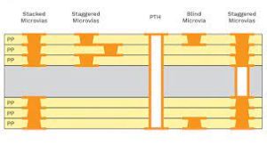
When deciding whether to use blind or buried vias, there are several factors that should be considered by the designer. One of the most important is whether the circuit board needs to make a connection between surface mount devices and internal layers. If so, blind via pcb are a better choice. Otherwise, buried vias would be more appropriate.
In order to create a blind via, the holes must be drilled after all of the layers have been laminated but before the outer layer has been etched and plated. The holes can be drilled mechanically or by laser. In either case, the ratio of hole diameter to depth (aspect ratio) must be greater than or equal to 1:12.
Once the holes have been drilled, they must then be filled with conductive material. There are several options for this process, including conductive epoxy and conductive silver. AE3030 is the most commonly used conductive paste for via fill. It offers excellent conductivity and performance, but it can be quite expensive compared to other via fills.
Can blind vias be filled with conductive or non-conductive materials?
It is crucial that the vias are plated with the proper material, as this will affect the overall quality of the finished product. Vias that are not plated correctly will be susceptible to corrosion, which can lead to poor connections and signal degradation. It is also critical that the copper plating is thick enough to prevent pinholes from forming in the finished product.
When designing a PCB that uses blind or buried vias, it is crucial to consult with the right manufacturer. The supplier should have the right equipment and experience to ensure that the design is fabricated properly. The correct manufacturing partner will also be able to provide the best pricing and fastest delivery times.
With the right PCB manufacturer, a project with blind or buried vias can be completed with ease and confidence. To get started, request a free quote today!
Blind vias are a crucial component in modern printed circuit boards (PCBs), providing pathways for electrical connections between layers while conserving valuable space. However, like any engineering solution, they come with their own set of considerations and potential reliability concerns.
Furthermore, blind vias introduce complexity to the PCB fabrication process. Traditional vias that span the entire thickness of the board can be manufactured using straightforward drilling and plating processes. However, blind vias require more intricate techniques, such as laser drilling or controlled-depth drilling, followed by specialized plating processes to ensure proper electrical conductivity. These additional steps increase manufacturing costs and the potential for errors, impacting both the reliability and affordability of the final product.